FPGAs provide massive gains in speed and processing capability owing to their ability to enable parallelization. And, with custom logic blocks that can be easily added and removed on the fly, they significantly lower long-term maintenance and equipment upgrade costs.
Those are just a few of the benefits an FPGA can bring to a business, so it’s no wonder they’re becoming so popular. However, FPGA technology is also very complex, and companies relying on legacy equipment may wonder if they lack the modernity to integrate this hardware.
The short answer is, they can, and here’s how the engineers at DornerWorks helped one do it.

A customer came to DornerWorks looking to replace their obsolete and now-unavailable Intel microprocessor with a VHDL based soft core IP equivalent.
Some of the reasons behind the choice to use a soft core replacement were:
Implementation of the new IP core presented many challenges that were not identified as risks in the initial assessment. This was partly due to FPGAs being relatively new to the implementation team, which was unfamiliar with the design methodology required to implement a complex IP core that was not targeted to any specific technology.
The first hint of an issue was found in the Vivado Synthesis Timing Summary.
Running a post synthesis timing report will provide a very good look at how ready a design (or IP core) is for implementation.
The Check Timing summary will provide information on unconstrained logic. The path reports will provide further insight if and to what magnitude the design is missing this first timing step.
In the case of this core, there were numerous unconstrained endpoint and very large setup and hold violations.
From the synthesized design we were able to quickly examine the problem timing paths. We immediately noticed that the core was not using any of the FPGA clocking resources for clocks that were generated by user logic.
Moreover, various unsynchronized domain crossings were found in the timing paths reports. Clearly, this IP core needed modifications before implementation in an UltraScale FPGA.
The first few questions that must be addressed:
To answer the first question, we wanted to isolate the IP core such that any exiting FPGA external logic that may itself have issues was not involved. The presence of a large setup and hold in the base FPGA design were also driving build times to over an hour. By isolating the IP core, the build times could be significantly reduced.
The ZedBoard proved to be an excellent platform for the IP core FPGA implementation. The Zynq 7020 FPGA was large enough and the evaluation board had sufficient I/O to allow stimulus to be generated for interrupts, timeout simulations, and other various needs.
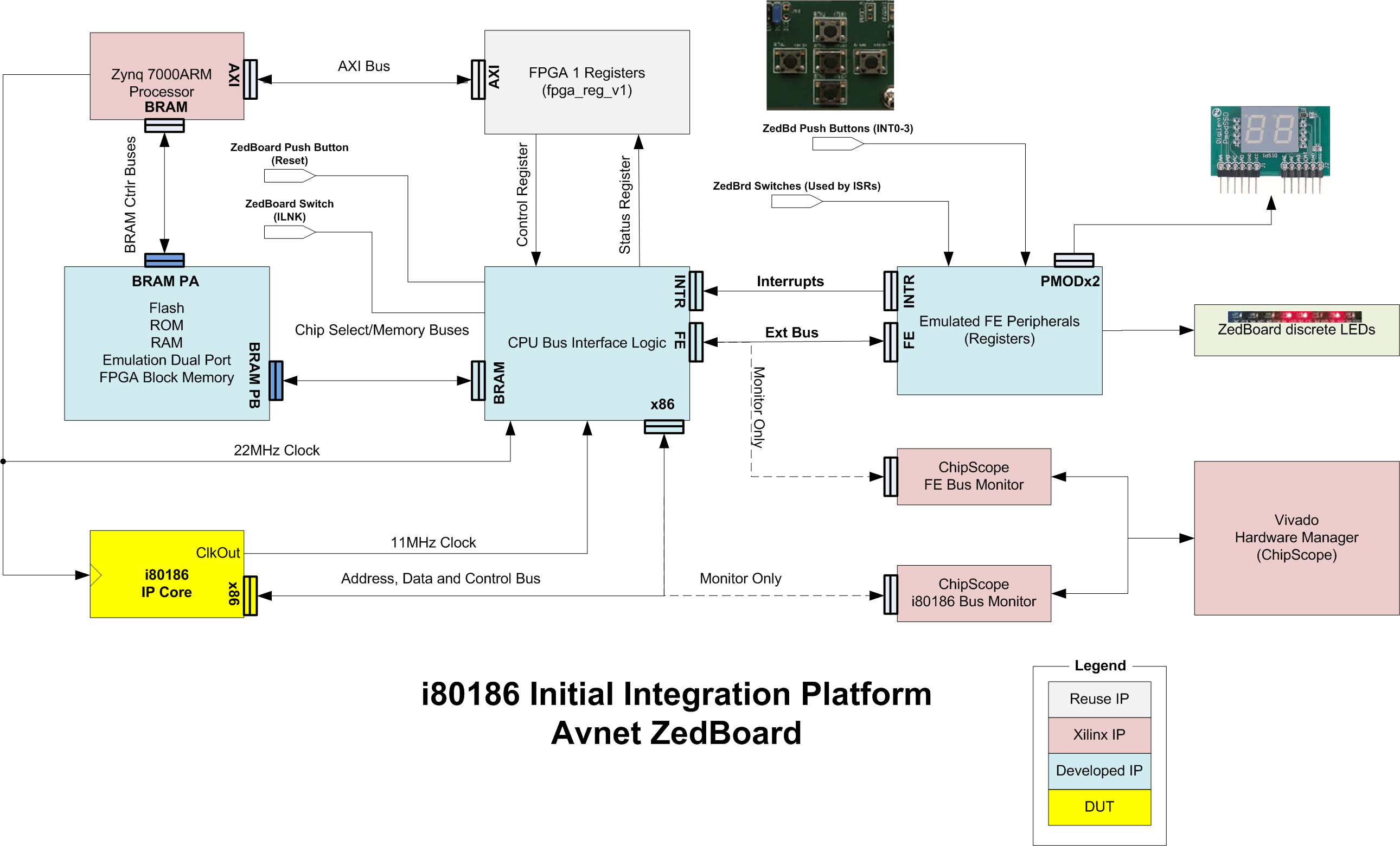
A small block diagram design was created that used dual ported block RAMs as ROM and RAM for the x86 processor. A standalone BSP ARM processing system was used to “hot configure” the x86 ROM with the test machine code. The standalone system is shown in figure 1. The Device Under Test is shown in yellow.
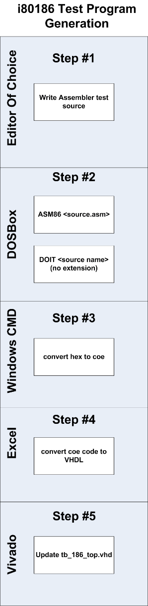
The next step was developing applications for the obsolete processor. Here, the diverse experience of the DornerWorks Engineering team came in to full use. One of our engineers was still familiar with the x86 processor assembly language and the needed build tools! The team was able to retrieve the tools from sources on the internet and stand up a build environment.
With some additional excel work a full x86 build environment was realized.
Figure 2 outlines the various steps taken to produce the BRAM coefficients data array for loading by the ARM.
There are a few options for source code. An old PL/M compiler exists but due to the desire to target exact functionality of the processor, the ASM86 Macro Assembler was chosen. Fortunately all the required related x86 utilities were also still available.
With the IP core isolated and all needed parts in place the core could be updated for implementation in a FPGA.